
Abstract
A feedback amplifier is one in which a portion of the output is fed back to the system input where it is combined with the input signal. The basic concept is shown in Fig. 7.1. At the amplifier input, the feedback signal which may be a voltage or current is combined with the input signal which is also a voltage or current through a summing or mixing network, and the resulting signal is passed into the amplifier system. The summing network is either a series circuit which mixes feedback voltage with source voltage or a shunt circuit which mixes feedback current with source current while the feedback network is most often a passive network, usually resistive.
Access this chapter
Tax calculation will be finalised at checkout
Purchases are for personal use only
Bibliography
J. Millman, C.C. Halkias, Integrated Electronics: Analog and Digital Circuits and Systems (McGraw Hill, New York, 1972)
A.S. Sedra, K.C. Smith, Microelectronic Circuits, 6th edn. (Oxford University Press, Oxford, 2011)
Author information
Authors and Affiliations
Problems
Problems
-
1.
Draw and label the equivalent voltage amplifier. Indicate the levels of the input and output resistances relative to the source and load resistances and show how negative feedback can be applied around the amplifier.
-
2.
Draw and label the equivalent current amplifier. Indicate the levels of the input and output resistances relative to the source and load resistances, and show how negative feedback can be applied around the amplifier.
-
3.
State four advantages of negative feedback in amplifiers, and show how such feedback can be implemented around a trans-resistance amplifier.
-
4.
Determine the amount of negative feedback in an operational amplifier having an open-loop gain of 110 dB and a closed-loop gain of 20 dB.
-
5.
Explain what is meant by “gain stabilization” in a negative feedback amplifier and why it is important in the design of such amplifiers.
-
6.
Show that the magnitude of the fractional change in the gain of an open-loop amplifier is reduced by a factor equal to the loop gain in the closed-loop amplifier.
-
7.
An amplifier with gain 1500 has a gain change of 15% due to aging. Calculate the change in gain of the feedback amplifier if the feedback factor β = 0.2.
-
8.
An amplifier with a transfer function \( A=\frac{k}{1+ jf/{f}_o} \) has a low-frequency open-loop gain of k = 120, 000 and an open-loop bandwidth of fo = 1 Hz. For a closed-loop gain of 100, calculate the closed-loop bandwidth of the amplifier.
-
9.
Show that negative feedback reduces the distortion in the output stage of an amplifier by a factor equal to the loop gain.
-
10.
Discuss the effect of negative feedback on the input and output resistances of the four classes of amplifiers.
-
11.
Show that the bandwidth of a feedback amplifier increases with the application of negative feedback.
-
12.
Evaluate the voltage gain, input resistance and output resistance for the voltage feedback amplifier in Fig. 7.61. For the transistors hfe = 120, hie = 5 k, hre = hoe = 0.
Fig. 7.61 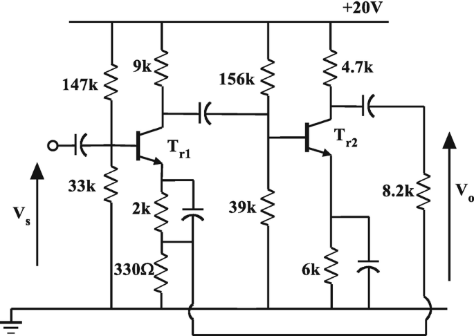
Diagram for Question 12
-
13.
For the current amplifier shown in Fig. 7.62, determine the closed-loop current gain, input resistance and output resistance. For the transistors hfe = 100, hie = 2.5k, hre = hoe = 0. Determine RS to give a voltage gain of 12.
Fig. 7.62 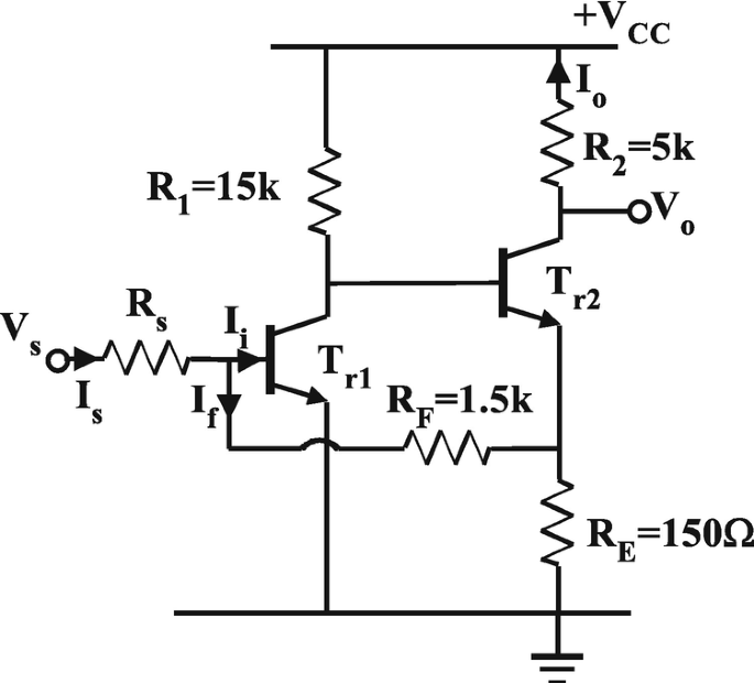
Diagram for Question 13
-
14.
For the transconductance amplifier of Fig. 7.63 determine the closed-loop transconductance GMf, the closed-loop input impedance and the closed-loop output impedance.
Fig. 7.63 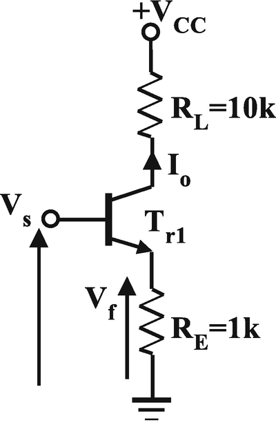
Diagram for Question 14
-
15.
For the trans-resistance amplifier of Fig. 7.64, determine RMf, Rif,Rof and the value of RS to give the system a voltage gain of 25. Use hfe = 120 andhie = 250.
Fig. 7.64 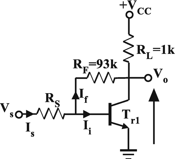
Diagram for Question 15
-
16.
For an operational amplifier with a GBP of 8 MHz, determine the closed-loop bandwidth if the closed-loop gain is 12.
-
17.
Design a four-transistor feedback amplifier using the topology in Fig. 7.40. Use a 24 volt symmetrical supply and small signal transistors with gain of 150. Design the system for a closed-loop gain of 8.
-
18.
Determine the open-loop voltage gain for the circuit mentioned in Question 17.
-
19.
Design a transistor amplifier with a gain of 8 using the configuration of Fig. 7.49. Use a 25 volt supply and transistors with current gain of 150.
-
20.
For the feedback amplifier shown in Fig. 7.65, determine the current in each transistor, assuming they are all matched.
Fig. 7.65 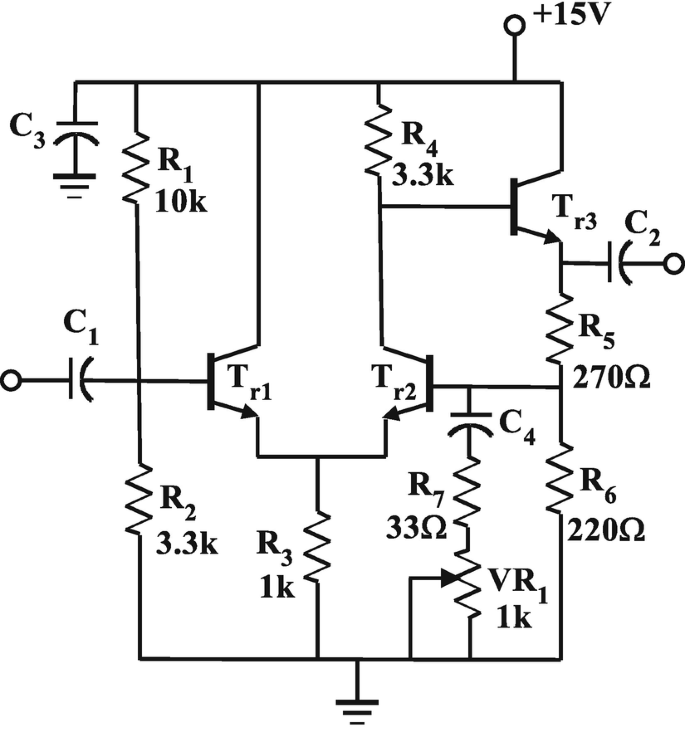
Diagram for Question 20


Rights and permissions
Copyright information
© 2021 Springer Nature Switzerland AG
About this chapter

Cite this chapter
Gift, S.J.G., Maundy, B. (2021). Feedback Amplifiers. In: Electronic Circuit Design and Application. Springer, Cham. https://doi.org/10.1007/978-3-030-46989-4_7
Download citation
DOI: https://doi.org/10.1007/978-3-030-46989-4_7
Published:
Publisher Name: Springer, Cham
Print ISBN: 978-3-030-46988-7
Online ISBN: 978-3-030-46989-4
eBook Packages: EngineeringEngineering (R0)