
Abstract
Knowledge of major circuit elements, their υ-i characteristics, and Ohm’s law (Chap. 2)
Access this chapter
Tax calculation will be finalised at checkout
Purchases are for personal use only
Notes
- 1.
Subtleties are often euphemism for “playing” around with the circuit, like redrawing the wire connections and rearranging the circuit elements. This is done to find simpler solution approaches.
- 2.
The first publication that discusses this equivalent circuit concept is actually due to Hans F. Mayer (1895–1980) who made the discovery in 1926 while a researcher at Siemens Company.
Author information
Authors and Affiliations
Appendices
Summary
Circuit analysis techniques: nodal/mesh analysis | ||
Nodal analysis |
| Based on KCL and Ohm’s law: \( \frac{V_1-{V}_{\mathrm{S}}}{R_1}+\frac{V_1-0\kern0.5em \mathrm{V}}{R_3}+\frac{V_1-{V}_2}{R_2}=0 \) \( \frac{V_2-{V}_{\mathrm{S}}}{R_5}+\frac{V_2-0\kern0.5em \mathrm{V}}{R_4}+\frac{V_2-{V}_1}{R_2}=0 \) |
Supernode |
| KCL for the supernode: \( \begin{array}{l}\frac{V_1-{V}_{\mathrm{S}}}{R_1}+\frac{V_1}{R_3}\\ {}+\frac{V_2}{R_4}+\frac{V_2-{V}_{\mathrm{S}}}{R_5}=0\end{array} \) plus KVL: \( {V}_2={V}_1+{V}_0 \) |
Mesh analysis |
| Based on KVL and Ohm’s law: \( {R}_1\left({I}_1-{I}_3\right)+{R}_3{I}_1+{R}_5\left({I}_1-{I}_2\right)=0 \) \( {R}_2\left({I}_2-{I}_3\right)+{R}_5\left({I}_2-{I}_1\right)+{R}_4{I}_2=0 \) \( -{V}_S+{R}_1\left({I}_3-{I}_1\right)+{R}_2\left({I}_3-{I}_2\right)=0 \) for meshes 1, 2, and 3 |
Supermesh |
| KVL for the supermesh: \( \begin{array}{l}{R}_1\left({I}_1-{I}_3\right)+{R}_3{I}_1+{R}_4{I}_2+\\ {}{R}_2\left({I}_2-{I}_3\right)=0\end{array} \) plus Eq. for mesh 3 and the KCL: \( {I}_1-{I}_2={I}_{\mathrm{S}} \) |
Circuit analysis techniques: source transformation theorem | ||
Source transformation theorem |
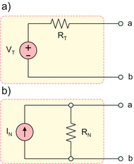
| Substitution of voltage source V T in series with resistance R T for current source I N with resistance R N: \( {R}_{\mathrm{N}}={R}_{\mathrm{T}} \) , \( {I}_{\mathrm{N}}=\frac{V_{\mathrm{T}}}{R_{\mathrm{T}}} \) \( {V}_{\mathrm{OC}}={V}_{\mathrm{T}} \) , \( {I}_{\mathrm{SC}}=\frac{V_{\mathrm{T}}}{R_{\mathrm{T}}} \) |
Circuit analysis techniques: Thévenin/Norton theorems/equivalents | ||
Thévenin and Norton theorems |
| Any linear network with independent sources, dependent linear sources, and resistances can be replaced by a simple equivalent network in the form: i. a voltage source V T in series with resistance R T; ii. a current source I N in parallel with resistance R N |
Summary of major circuit analysis methods (linear circuits) – Superposition theorem (previous chapter); – Nodal/mesh analysis (this chapter); – Source transformation theorem (this chapter); – Thévenin and Norton equivalent circuits (this chapter) | ||
Linear networks: measurements/equivalence | ||
Method of short/open circuit |
| – Two arbitrary linear networks are equivalent when their V OC and I SC coincide. – This method is also used for nonlinear circuits |
Linear networks: maximum power theorem | ||
Maximum power theorem (load matching) |
| – Power delivered to the load is maximized when \( {R}_{\mathrm{L}}={R}_{\mathrm{T}} \); – For high-frequency circuits it also means no “voltage/current wave reflection” from the load |
Linear networks: maximum power efficiency | ||
Power efficiency is maximized when the load resistance is very high (load bridging) |
| Power transfer efficiency: \( E=\frac{P_{\mathrm{L}}}{P}=\frac{R_{\mathrm{L}}}{R_{\mathrm{T}}+{R}_{\mathrm{L}}} \) |
Linear networks: dependent sources and negative equivalent resistance | ||
Equivalent resistances of basic linear networks with dependent sources |
| Case a): \( {R}_{\mathrm{T}}=\frac{R}{1-A} \) Case b): \( {R}_{\mathrm{T}}=R-Z \) Case c): \( {R}_{\mathrm{T}}=\frac{R}{1-GR} \) Case d): \( {R}_{\mathrm{T}}=R\left(1-A\right) \) Equivalent resistance may become negative |
Nonlinear networks: four basic topologies | ||
Basic nonlinear circuits |
| – Linear voltage source connected to a nonlinear load (diode circuit); – Linear current source connected to a nonlinear load; – Nonlinear voltage source connected to a linear load; – Nonlinear current source connected to a linear load (photovoltaic circuit) |
Nonlinear networks: circuit analysis via load line method | ||
Load line method |
| Solution: The load line (υ-i characteristic of the linear source, which is \( I=\frac{V_{\mathrm{T}}-V}{R_{\mathrm{T}}} \)) intersects the υ-i characteristic of the nonlinear load, I (V) |
Nonlinear networks: iterative solution | ||
Finding the intersection point iteratively | For the circuit in the previous row: \( I(V)=\frac{V_{\mathrm{T}}-V}{R_{\mathrm{T}}}\Rightarrow {V}^{n+1}={I}^{-1}\left(\frac{V_{\mathrm{T}}-{V}^n}{R_{\mathrm{T}}}\right),\kern0em n=0,\kern0.5em 1,\kern0.5em \dots \) | Implicit scheme: initial guess V 0may be 0 V |
Nonlinear networks: finding resistive load for maximum power extraction | ||
Finding maximum load power for the equivalent model of a solar cell |
| Load power is computed as \( {P}_{\mathrm{L}}=V\times I(V) \). Then, it is maximized, which is equivalent to solving equation: \( \frac{d{P}_{\mathrm{L}}}{dV}(V)=0 \) for unknown voltage V |


Some useful facts about power extraction from solar cells/modules | |||
Typical values of open-circuit voltage V OC and photocurrent density J P of a c-Si cell | Crystalline silicon or c-Si cell: \( {V}_{\mathrm{OC}}\approx 0.6\kern0.5em \mathrm{V} \); \( {J}_{\mathrm{P}}\approx 0.03\ \mathrm{A}/{\mathrm{cm}}^2 \) | ||
– Open-circuit module voltage is N times the cell voltage, \( N\cdot {V}_{\mathrm{OC}} \) – Short-circuit module current I SC is the cell short-circuit current \( {I}_{\mathrm{SC}}=A{J}_{\mathrm{P}} \) where A is cell area |
| ||
Typical values of maximum-power parameters and fill factor for c-Si cells/modules; the load resistance must be \( {R}_{\mathrm{L}}={V}_{\mathrm{MP}}/{I}_{\mathrm{MP}} \) | \( {\left.F\right|}_{\mathrm{module}}=\frac{V_{\mathrm{MP}}{I}_{\mathrm{MP}}}{V_{\mathrm{OC}}{I}_{\mathrm{SC}}}\approx {\left.F\right|}_{\mathrm{cell}} \) (for low-loss modules) \( {V}_{\mathrm{MP}}\approx 0.8\kern0.1em {V}_{\mathrm{OC}},\kern0.75em {I}_{\mathrm{MP}}\approx 0.9{I}_{\mathrm{SC}},\kern0.5em F\approx 0.72 \) | ||
Lossless single-diode model of a solar cell: \( {I}_{\mathrm{P}}=A{J}_{\mathrm{P}} \)—photocurrent (A); A—cell area (cm2); V T—thermal volt. (0.0257 V); n—ideality factor (\( 1<n<2 \)); \( {I}_{\mathrm{S}}\approx {I}_{\mathrm{P}} \exp \left(-\frac{V_{\mathrm{OC}}}{n{V}_{\mathrm{T}}}\right) \) (A) |
\( I={I}_{\mathrm{P}}-{I}_{\mathrm{S}}\left[ \exp \left(\frac{V}{n{V}_{\mathrm{T}}}\right)-1\right] \) | ||
Maximum-power analytical solution for lossless single-diode model of a solar cell | \( {V}_{\mathrm{MP}}\approx {V}_{\mathrm{OC}}-n{V}_{\mathrm{T}} \ln \left(1+\frac{V_{\mathrm{OC}}}{n{V}_{\mathrm{T}}}\right) \), \( {I}_{\mathrm{MP}}={I}_{\mathrm{SC}}\left(1-\frac{n{V}_{\mathrm{T}}}{V_{\mathrm{MP}}}\right) \) | ||


Problems
2.1 4.1 Nodal/Mesh Analysis
4.1.2 Nodal analysis
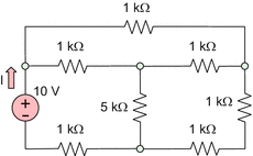
Problem 4.1
-
A.
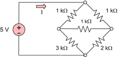
Using the nodal analysis, determine the supply current I for the circuit shown in the figure.
-
B.
Show the current directions for every resistance in the circuit.

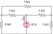
Problem 4.2
-
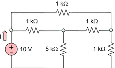
A.
Using the nodal analysis, determine the total circuit current I for the circuit shown in the following figure.
-
B.
Show the current directions for every resistance in the circuit.

Problem 4.3
Introduce the ground termination, write the nodal equations, and solve for the node voltages for the circuit shown in the following figure. Calculate the current I shown in the figure.

Problem 4.4
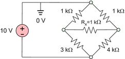
Introduce the ground termination, write the nodal equations, and solve for the node voltages for the circuit shown in the figure. Calculate the current through the resistance R x and show its direction in the figure.

Problem 4.5
For the circuit shown in the following figure,
-
1.
Determine current i x through resistance R x .
-
2.
Show its direction on the figure.

Problem 4.6
For the circuit shown in the following figure,
-
A.
Write nodal equations and solve for the node voltages . Then, find the value of i 1.
-
B.
Could this problem be solved in another (simpler) way?

Problem 4.7
-
A.
Write the nodal equations and solve for the node voltages for the circuit shown in the following figure. Then, find the value of i 1.
-
B.
Use MATLAB or other software of your choice for the solution of the system of linear equations; attach the code to the solution.

Problem 4.8
The following figure shows the DC equivalent of a residential three-wire system, which operates at 240 V rms (do not confuse it with the three-phase system, which carries a higher current). Two 120-V rms power supplies are connected as one dual-polarity power supply, i.e., in series. The 10-Ω load and the 20-Ω load are those driven by the two-wire (and one ground) standard wall plug with 120 V rms—the lights, a TV, etc. The 6-Ω load consumes more power and it is driven with 240 V rms using a separate bigger wall plug (+/− and neutral (not shown))—the stove, washer, dryer, etc. Determine the power delivered to each load. Hint: Use a calculator or software of your choice for the solution of the system of linear equations (MATLAB is recommended).

4.1.3 Supernode
Problem 4.9
Introduce the ground terminal, write the nodal equations, and solve for the node voltages for the circuit shown in the figure. Calculate the current I shown in the figure.

Problem 4.10
Introduce the ground terminal, write the nodal equations, and solve for the node voltages for the circuit shown in the figure. Calculate the current I shown in the figure.

4.1.4 Mesh analysis
4.1.5 Supermesh
Problem 4.11
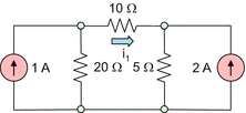
For the circuit shown in the figure, determine current i 1
-
A.
Using the mesh analysis
-
B.
Using the nodal analysis
Which method is simpler?

Problem 4.12
For the circuit shown in the figure, determine voltage V x
-
A.
Using the mesh analysis
-
B.
Using the nodal analysis
Which method appears to be simpler?

Problem 4.13
For the circuit shown in the figure
-
A.
Determine the circuit current I using either the nodal analysis or the mesh analysis.
-
B.
Explain your choice for the selected method.

Problem 4.14
For the circuit shown in the figure, determine its equivalent resistance between terminals a and b. Hint: Connect a power source and use a mesh-current analysis or the nodal analysis.

Problem 4.15
For the circuit shown in the figure, determine the current i 1 of the 20-V voltage source.

Problem 4.16
Determine voltage across the current source for the circuit shown in the figure that follows using the mesh analysis and the supermesh concept.

2.2 4.2 Generator Theorems
4.2.1 Equivalence of Active One-Port Networks . Method of Short/Open Circuit
Problem 4.17
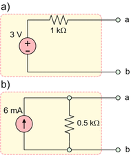
A linear active network with two unknown circuit elements measures \( {V}_{\mathrm{OC}}=5\kern0.5em \mathrm{V} \), \( {I}_{\mathrm{SC}}=10\kern0.5em \mathrm{m}\mathrm{A} \).
-
A.
Determine parameters V T, R T and I N, R N of two equivalent networks shown in the figures below.
-
B.
Could you identify which exactly network is it?

Problem 4.18
Given two networks shown in the figure that follows:
-
A.
Determine their open-circuit voltage V OC and short-circuit current I SC for each of them.
-
B.
Are the networks equivalent?

4.2.2 Application example: reading and using data for solar panels
Problem 4.19
The area of a single cell in the 10-W BSP-1012 Power Up c-Si panel is ~22 cm2. Predict:
-
A.
Open-circuit voltage of the solar cell, V OC
-
B.
Photocurrent density of the cell, J P
-
C.
Short-circuit current of the cell, I SC
Compare the above value with the value \( {I}_{\mathrm{SC}}=0.66\kern0.5em \mathrm{A} \) reported by the manufacturer.
Problem 4.20
The area of a single cell in the 175-W BP Solar SX3175 c-Si panel is 156.25 cm2. Predict:
-
A.
Open-circuit voltage of the solar cell, V OC
-
B.
Photocurrent density of the cell, J P
-
C.
Short-circuit current of the cell, I SC
Compare the above value with the value \( {I}_{\mathrm{SC}}=5.1\;\mathrm{A} \) reported by the manufacturer. What value should the photocurrent density have in order to exactly match the short-circuit current reported by the manufacturer?
Problem 4.21
Are the solar cells in the solar module connected in parallel or in series? Why is one particular connection preferred?
Problem 4.22
You are given three c-Si solar cells shown in the figure that follows, each of area A/3. Draw wire connections for a cell bank, which has the performance equivalent to that of a large solar cell with the area A.

Problem 4.23
Individual solar cells in the figure to the previous problem are to be connected into a standard solar module. Draw the corresponding wire connections.
Problem 4.24
A 10-W BSP1012 PV c-Si module shown in the figure has 36 unit cells connected in series, the short-circuit current of 0.66 A, and the open-circuit voltage of 21.3 V.

-
A.
Estimate the area of the single solar cell using the common photocurrent density value for c-Si solar cells.
-
B.
Estimate the open-circuit voltage for the single cell.
Problem 4.25
A 20-W BSP2012 PV c-Si module shown in the figure has 36 unit cells connected in series, the short-circuit current of 1.30 A, and the open-circuit voltage of 21.7 V.

-
A.
Estimate the area of the single solar cell using the common photocurrent density value for c-Si solar cells.
-
B.
Estimate the open-circuit voltage for the single cell.
Problem 4.26
A c-Si solar module is needed with the open-circuit voltage of 10 V and the short-circuit current of 1.0 A. A number of individual solar cells are available; each has the area of 34 cm2, the open-circuit voltage of 0.5 V, and the short-circuit current of 1.0 A. Identify the proper module configuration (number of cells) and estimate the module’s approximate size.
Problem 4.27
A c-Si solar module is needed with the open-circuit voltage of 12 V and the short-circuit current of 3.0 A. A number of individual solar cells are available; each has the area of 34 cm2, the open-circuit voltage of 0.5 V, and the short-circuit current of 1.0 A. Identify the proper module configuration (number of cells) and estimate the module’s approximate size.
4.2.3 Source Transformation Theorem
Problem 4.28
Find voltage V in the circuit shown in the figure that follows using source transformation.

Problem 4.29
The circuit shown in the following figure includes a current-controlled voltage source. Find current i x using source transformation.

Problem 4.30
The circuit shown in the following figure includes a voltage-controlled voltage source. Find voltage υ x using source transformation.

Problem 4.31
Repeat the previous problem for the circuit shown in the figure below.

4.2.4 Thévenin’s and Norton’s Theorems
Problem 4.32
Find:
-
1.
Thévenin (or equivalent) voltage
-
2.
Thévenin (or equivalent) resistance
for the two-terminal network shown in the figure that follows. Assume three 9-V sources separated by resistances of 1 Ω each.

Problem 4.33
Find:
-
1.
Thévenin (or equivalent) voltage
-
2.
Thévenin (or equivalent) resistance
for the two-terminal network shown in the figure that follows (three practical voltage sources in series) when

Problem 4.34
Find:
-
1.
Thévenin (or equivalent) voltage;
-
2.
Thévenin (or equivalent) resistance
for the two-terminal networks shown in the following figures.

Problem 4.35
Find:
-
1.
Thévenin voltage
-
2.
Thévenin resistance
for the two-terminal network shown in the following figure when
\( {R}_1={R}_2={R}_3=1\mathrm{k}\Omega, {V}_{S1}={V}_{S2}=10\kern0.5em \mathrm{V}. \)

Problem 4.36
A two-terminal network shown in the figure is a starting section of a ladder network used for digital-to-analog conversion. Express:
-
1.
Thévenin (or equivalent) voltage
-
2.
Thévenin (or equivalent) resistance
in terms of (digital) voltage D 0 and resistance R.

Problem 4.37
A two-terminal circuit network in the figure is a two-bit ladder network used for digital-to-analog conversion. Express parameters of the corresponding Norton equivalent circuit in terms of (digital) voltages D 0, D 1 and resistance R.

Problem 4.38
A two-terminal network shown in the figure is a four-bit ladder network used for digital-to-analog conversion. Express:
-
1.
Thévenin ( or equivalent) voltage
-
2.
Thévenin (or equivalent) resistance
in terms of four (digital) voltages D 0, D 1, D 2, D 3 and resistance R.

Problem 4.39
Determine the Norton equivalent for the circuit shown in the figure. Express your result in terms of I and R.

Problem 4.40
Each of three identical batteries is characterized by its Thévenin equivalent circuit with \( {V}_{\mathrm{T}}=9\ \mathrm{V} \) and \( {R}_{\mathrm{T}}=1\ \Omega \). The batteries are connected in parallel. The parallel battery bank is again replaced by its Thévenin equivalent circuit with unknown V TBank and R TBank. Find those parameters (show units). Hint: This is a tricky problem; double-check the connecting nodes when drawing the circuit diagram.
Problem 4.41
Establish Thévenin and Norton equivalent circuits for the network shown in the following figure.

4.2.5 Application Example: Generating Negative Equivalent Resistance
Problem 4.42
Establish the equivalent (Thévenin) resistance for the network shown in the following figure. Carefully examine the sign of the equivalent resistance.

Problem 4.43
Derive the equivalent (Thévenin) resistance for the networks shown in the figure that follows (confirm Fig. 4.16 of the main text).

4.2.6 Summary of Circuit Analysis Methods
Problem 4.44
Solve the circuits shown in the following figure—determine current I (show units). You can use any of the methods studied in class:
-
Superposition theorem
-
Nodal/mesh analysis
-
Source transformation theorem
-
Thévenin and Norton equivalent circuits
Attempt to apply two different methods of your choice to every circuit.

Problem 4.45
Solve the circuits shown in the following figure—determine unknown voltage V or current I (show units). You can use any of the methods studied in class:
-
Superposition theorem
-
Nodal/mesh analysis
-
Source transformation theorem
-
Thévenin and Norton equivalent circuits

2.3 4.3 Power Transfer
4.3.1 Maximum Power Transfer
4.3.2 Maximum Power Efficiency
Problem 4.46
A deep-cycle marine battery is modeled by an ideal voltage source of 24 V in series with a 1-Ω resistance shown in the figure that follows. The battery is connected to a load, and the load’s resistance, R L, needs to be optimized. Power delivered to the load has a maximum at exactly one value of the load resistance. Find that value and prove your answer graphically using software of your choice (MATLAB is recommended).

Problem 4.47
A power supply for an electric heater can be modeled by an ideal voltage source of unknown voltage in series with the internal resistance \( {R}_{\mathrm{T}}=4\kern0.5em \Omega \).
-
A.
Can you still determine when the power delivered to a load (a heating spiral with resistance R L) is maximized?
-
B.
Does the answer depend on the source voltage?
Problem 4.48
For the circuit shown in the figure, when is the power delivered to the load maximized?

Problem 4.49
A battery can be modeled by an ideal voltage source V T in series with a resistance R T.

-
1.
For what value of the load resistance R L is the power delivered to the load maximized?
-
2.
What percentage of the power taken from the voltage source V T is actually delivered to a load (assuming R L is chosen to maximize the power delivered)?
-
3.
What percentage of the power taken from the voltage source V T is delivered to a load when \( {R}_{\mathrm{L}}=0.1{R}_{\mathrm{T}} \)?
Problem 4.50
A micro-power photovoltaic device can be modeled under certain conditions as an ideal current power source and a resistance in parallel—see the figure that follows. At which value of the load resistance, R L, is the power delivered to the load maximized?

Problem 4.51
A low-cost polycrystalline Power Up BSP1-12 1-W solar panel lists ratings for the output voltage and current, which give maximum load power: V L max = 17.28 V, I L max = 0.06 A. Based on these cell specifications, which value of the equivalent resistance should the load to be connected to the solar cell have for maximum power output?
Problem 4.52
The solar panel from the previous problem generates a significant voltage of ~13 V in a classroom without direct sunlight, but the resulting current is small, ~1 mA.
-
A.
Now, what value of the equivalent resistance should the load have for maximum power output?
-
B.
How is the maximum load power different, compared to the previous problem?
Problem 4.53
The heating element of an electric cooktop has two resistive elements, \( {R}_1=50\ \Omega \) and \( {R}_2=100\ \Omega \), that can be operated separately, in series, or in parallel from a certain voltage source that has a Thévenin (rms) voltage of 120 V and internal (Thévenin) resistance of 30 Ω. For the highest power output, how should the elements be operated? Select and explain one of the following: 50 Ω only, 100 Ω only, series, or parallel.
Problem 4.54
You are given two speakers (rated at 4 Ω and 16 Ω, respectively) and an audio amplifier with the output resistance(impedance) equal to 8 Ω.

-
A.
Sketch the circuit diagram that gives the maximum acoustic output with the available components. Explain your choice.
-
B.
Sketch the circuit diagram for the maximum power efficiency. Explain your choice.
4.3.4 Application Example: Maximum Power Extraction from Solar Panel
Problem 4.55
-
A.
Describe in your own words the meaning of the fill factor of a solar cell (and solar module).
-
B.
A 200-W GE Energy GEPVp-200 c-Si panel has the following reading on its back: \( {V}_{\mathrm{OC}}=32.9\kern0.5em \mathrm{V} \), \( {I}_{\mathrm{SC}}=8.1\kern0.5em \mathrm{A} \), \( {V}_{\mathrm{MP}}=26.3\kern0.5em \mathrm{V} \), and \( {I}_{\mathrm{MP}}=7.6\kern0.5em \mathrm{A} \). What is the module fill factor? What is approximately the fill factor of the individual cell?
Problem 4.56
Using two Web links
http://www.affordable-solar.com/,
identify the solar panel that has the greatest fill factor to date.
Problem 4.57
A 10-W BSP1012 PV c-Si module shown in the figure has 36 unit cells connected in series, the short-circuit current of 0.66 A, and the open-circuit voltage of 21.3 V. The maximum power parameters are \( {V}_{\mathrm{MP}}=17.3\kern0.5em \mathrm{V} \) and \( {I}_{\mathrm{MP}}=0.58\kern0.5em \mathrm{A} \).

-
A.
Estimate the area of the single solar cell using the common photocurrent density value for c-Si solar cells (show units).
-
B.
Estimate the open-circuit voltage for the single cell.
-
C.
Estimate the fill factor of the module and of the cell.
-
D.
Estimate the value of the equivalent load resistance R required for the maximum power transfer from the module to the load.
Problem 4.58
A 20-W BSP2012 PV c-Si module shown in the figure has 36 unit cells connected in series, the short-circuit current of 1.30 A, the open-circuit voltage of 21.7 V, the maximum power voltage V MP of 17.3 V, and the maximum power current I MP of 1.20 A. Repeat the four tasks of the previous problem.

Problem 4.59
A REC SCM220 220-watt 20V c-Si solar panel shown in the figure has the following readings on the back: the short-circuit current I SC of ~8.20 A, the open-circuit voltage V OC of ~36.0 V, the maximum power voltage V MP of ~28.7 V, and the maximum power current I MP of ~7.70 A. Repeat the four tasks of problem 4.57.

Problem 4.60
A 14.4-W load (a DC motor) rated at 12 V is to be driven by a solar panel. A c-Si photovoltaic sheet material is given, which has the open-circuit voltage of 0.6 V and the photocurrent density of \( {J}_{\mathrm{P}}=0.03\ \mathrm{A}/{\mathrm{cm}}^2 \).

Outline parameters of a solar module (number of cells, cell area, and overall area) which is capable of driving the motor at the above conditions and estimate the overall panel size.
Problem 4.61
A custom 100-W load (a DC motor) rated at 24 V is to be driven by a solar panel. A c-Si photovoltaic sheet material is given, which has the open-circuit voltage of 0.6 V and the photocurrent density of \( {J}_{\mathrm{P}}=0.03\ \mathrm{A}/{\mathrm{cm}}^2 \). Outline parameters of a solar module (number of cells, cell area, and overall area) which is capable of driving the motor at the above conditions and estimate the overall panel size.
Problem 4.62
You are given: the generic fill factor \( F=0.72 \) for a c-Si solar panels, the generic open-circuit voltage \( {V}_{\mathrm{OC}}=0.6\mathrm{V} \) of a c-Si cell, and the generic photocurrent density \( {J}_{\mathrm{P}}=0.03\kern0.5em \mathrm{W}/{\mathrm{cm}}^2 \).
-
A.
Derive an analytical formula that expresses the total area A module in cm2 of a solar panel, which is needed to power a load, in terms of the required load power P L.
-
B.
Test your result by applying it to the previous problem.
Problem 4.63
You are given a low-cost low-power flexible (with the thickness of 0.2 mm) a-Si laminate from PowerFilm, Inc., with the following parameters: a fill factor of \( F=0.61 \), a single-cell open-circuit voltage of \( {V}_{\mathrm{OC}}=0.82\kern0.5em \mathrm{V} \), and a photocurrent density of \( {J}_{\mathrm{P}}=0.0081\kern0.5em \mathrm{A}/{\mathrm{cm}}^2 \).
-
A.
Derive an analytical formula that expresses the total module area A module in cm2, which is needed to power a load, in terms of the required load power P L.
-
B.
Compare your solution with the solution to the previous problem.


2.4 4.4 Analysis of Nonlinear Circuits. Generic Solar Cell
4.4.1 Analysis of Nonlinear Circuits: Load Line Method
4.4.2 Iterative Solution for Nonlinear Circuits
Problem 4.64
A circuit shown in the following figure contains a nonlinear passive element. Using the load line method, approximately determine the voltage across the element and the current through it for the two types of the υ-i characteristic, respectively.

Problem 4.65
A circuit shown in the following figure contains a nonlinear passive element as part of a current source. Using the load line method, approximately determine the voltage across the element and the current through it for the υ-i characteristic of the nonlinear element shown in the same figure.

Problem 4.66
Repeat the previous problem for the circuit shown in the following figure.

Problem 4.67
A circuit shown in the following figure contains a nonlinear passive element. The υ-i characteristic of the nonlinear element (the ideal Shockley diode) is
Using the iterative solution, determine the voltage across the element and the current through it.

Problem 4.68
Repeat the previous problem for the circuit shown in the following figure. The υ-i characteristic of the nonlinear element is the same.

4.4.3 Application Example: Solving the Circuit for a Generic Solar Cell
Problem 4.69
The I(V) dependence for a resistive load in a circuit is shown in the figure that follows.

-
A.
At which value of the load voltage is the power delivered to the load maximized?
-
B.
What is the related value of load resistance?
Problem 4.70
A hypothetic thermoelectric engine developed by the US Navy has the I (V) dependence shown in the figure that follows.

-
1.
At which value of the load voltage is the power, P L, delivered to the load maximized?
-
2.
What is the related value of load resistance for maximum power transfer?
Problem 4.71
Estimate the values of V MP and I MP versus V OC and I SC for a set of generic c-Si solar cells. Every cell has \( {V}_{\mathrm{T}}=0.026\;\mathrm{V} \) (room temperature of 25 °C) and \( {V}_{\mathrm{OC}}=0.6\kern0.5em \mathrm{V} \). The ideality factor n in Eqs. (4.43)–(4.45) is allowed to vary over its entire range as shown in the table that follows.
n | V MP/V OC,% | I MP/I OC,% | F |
1.00 | |||
1.25 | |||
1.50 | |||
1.75 | |||
2.00 |
Rights and permissions
Copyright information
© 2016 Springer International Publishing Switzerland
About this chapter
Cite this chapter
N. Makarov, S., Ludwig, R., Bitar, S.J. (2016). Circuit Analysis and Power Transfer. In: Practical Electrical Engineering. Springer, Cham. https://doi.org/10.1007/978-3-319-21173-2_4
Download citation
DOI: https://doi.org/10.1007/978-3-319-21173-2_4
Publisher Name: Springer, Cham
Print ISBN: 978-3-319-21172-5
Online ISBN: 978-3-319-21173-2
eBook Packages: EngineeringEngineering (R0)