
Abstract
In Chap. 4, we have introduced the basic concepts and formalism of quantum mechanics. In Chap. 0, we have determined the energy spectrum, or energy-momentum or E–k relations, for electrons in a crystal which governs their interaction with external forces and fields. Moreover, we saw that the quantum behavior of particles is best observed in small, typically nanometer scale (one billionth of a meter or 10−9 m) dimension structures, as illustrated in the example of a particle in a 1D box.
Access this chapter
Tax calculation will be finalised at checkout
Purchases are for personal use only
References
Bockrath M, Cobden DH, Lu J, Rinzler AG, Smalley RE, Balents L, McEuen PL (1999) Luttinger liquid behaviour in carbon nanotubes. Lett Nat 397:598–601
Shockley W (1951) U.S. Patent 2,569,347
Further Reading
Ahmed H (1986) An integration microfabrication system for low dimensional structures and devices. In: Kelly MJ, Weisbuch C (eds) The physics and fabrication of microstructures and microdevices. Springer, Berlin, pp 435–442
Ashcroft NW, Mermin ND (1976) Solid state physics. Holt, Rinehart, Winston, New York
Bassani F, Pastori Parravicini G (1975) Electronic states and optical transitions in solids, Chap. 6. Pergamon, New York
Bastard G (1988) Wave mechanics applied to semiconductor Heterostructures. Halsted Press, New York
Beaumont SP (1992) Quantum wires and dots-defect related effects. Phys Scr T45:196–199
Chuang SL (1995) Physics of optoelectronic devices. John Wiley & Sons, Inc., New York
Davies JH (1998) The physics of low dimensional semiconductors: an introduction. Cambridge University Press, New York
Dingle R Confined carrier quantum states in ultrathin semiconductor heterostructures. In: Queisser HJ (ed) Feskorperproblem XV, pp 21–48
Einspruch NG, Frensley WR (1994) Heterostructures and quantum devices. Academic Press, London
Hasko DG, Potts A, Cleaver JR, Smith C, Ahmed H (1988) Fabrication of sub-micrometer free standing single crystal GaAs and Si structures for quantum transport studies. J Vac Sci Technol B 6:1849–1851
Rosencher E, Vinter B (2002) Optoelectronics. Cambridge University Press, Cambridge
Scherer A, Jewell J, Lee YH, Harbison J, Florez LT (1989) Fabrication of microlasers and microresonator optical switches. Appl Phys Lett 55:2724–2726
Sze S (1981) Physics of semiconductor devices, 2nd edn. John Wiley & Sons, Inc., New York
Tewordt M, Law V, Kelly M, Newbury R, Pepper M, Peacock C (1990) Direct experimental determination of the tunneling time and transmission probability of electrons through a resonant tunneling system. J Phys Condens Matter 2:896–899
Vasko FT, Kuznetsov AV (1999) Electronic states and optical transitions in semiconductor heterostructures. Springer, New York
Weisbuch C, Vinter B (1991) Quantum semiconductor structures. Academic Press, New York
Author information
Authors and Affiliations
Problems
Problems
-
1.
In this chapter, we used the effective mass of the electron in the Schrödinger equation. Explain why it was necessary to do so, whereas it was not necessary in the infinite and finite potential well in Chap. 4.
-
2.
Give an expression (an integral) for the total number of electrons in the conduction band of a bulk three-dimensional semiconductor and then in the first subband of a quantum well of width L in terms of the density of states and the Fermi function (assume box eigenstates in the confined direction). If at T = 0 K we dope the first subband in the conduction band and we fill all the states in the first subband, how many electrons do we need per unit area?
-
3.
Consider a 50 Å GaAs and 300 Å Al0.6Ga0.4As layers forming a quantum well structure.
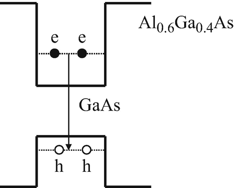

The electrons are all located at the first energy state (e), and holes are at (h). The general expression of the first energy state is determined as E1 = ℏ2π2/2m∗a2, where a is the width of the quantum well and m* is the effective mass of the particle considered (for holes, consider the heavy-hole effective mass).
What is the photon energy of the light emitted when the electron and the hole recombine as shown in the above figure?
-
4.
Let us assume a quantum dot which is spherical. The electrons or holes are confined at energy states with the following expression: Enl = (ℏ2/2m∗)(αnl/R)2, where m* is the effective mass of the electron or hole and the value of αnl is given by α10 = π, α11 = 4.49, α12 = 5.76, α20 = 6.28, α21 = 7.72, and α22 = 9.09. Now consider the very small GaAs quantum dots of radius 10 nm. If the electron drops from the second state (α11) to the first state (α10), what is the photon energy of the light emitted from this transition?
Draw the energy diagram for GaAs quantum dots with radius 5 nm, 10 nm, and 15 nm. How does the first energy state change as a function of radius?
-
5.
Density of States of an Ideal Two-Dimensional Electron Gas
Using the infinite barrier approximation, derive an expression for the density of states for electrons in a quantum well in terms of the well width L and electron effective mass m*.
-
6.
Fermi Energy of an Ideal Two-Dimensional Electron Gas
Consider a structure consisting of two GaAs quantum wells that have been grown far apart in AlxGa1-xAs with the same Al composition x (x ≤ 0.3). In well A the GaAs thickness is L, while in well B, it is 2L. Now, approximate the conduction bands in wells A and B by ideal quantum wells between infinitely high potential barriers. Suppose that the quantum wells contain electrons and that both wells have the same Fermi energy,\( {E}_{\mathrm{F}}=3{F}_1^{\mathrm{A}} \) where \( {E}_1^{\mathrm{A}} \) is the lowest quantized energy level in well A.
-
(a)
How many subbands in each well contain electrons at zero temperature?
-
(b)
What is the two-dimensional charge density NA and NB in each well?
Give the answer in terms of known physical quantities such as ℏ and L.
-
(a)
-
7.
The Graphic of the Two-Dimensional Density of States
Figure 15 shows the density of states of a quantum well. The confinement energy of the lowest level (E1) is 17 meV, and the first excited state (E2) has a confinement energy of 30 meV. The Fermi level is located 50 meV above the bottom of the conduction band. Determine the number of electrons contained in the well.
-
8.
The two-dimensional potential which confines the electrons in a quantum wire made of GaAs is assumed to be parabolic, and the subband separation is given as ℏω0 = 12 meV. If the Fermi energy is EF = 37 meV as measured from the bottom of the lowest subband, calculate the number of electron per unit length at 0 K including spin degeneracy.
-
9.
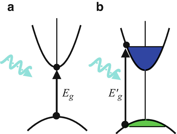
The Moss-Burstein Shift in Absorption Spectra
The “band filling” or Moss-Burstein shift effect occurs in all heavily doped three-dimensional semiconductors. It is a consequence of the fact that electrons are fermions, and therefore it is impossible (by the Pauli exclusion principle) to optically excite an electron into a same spin k-state, which is already occupied. In the case of strongly degenerate n+-doped sample, this has the effect of prohibiting any interband transition into electron states below the Fermi energy leading to an upward shift in the effective absorption edge, \( {E}_{\mathrm{g}}^{\prime } \) (see figure below). The Moss-Burstein shift (ΔE) is defined as the difference between the effective absorption edge and the energy gap (Eg) of the material, i.e., \( \Delta E={E}_{\mathrm{g}}^{\prime }-{E}_{\mathrm{g}} \).
-
(a)
Calculate the Burstein shift in the absorption edge of a direct semiconductor with parabolic bands due to the heavy doping (n-type) at very low temperature (T ≈ 0 K). The carrier concentration is ne. Neglect excitons. Note that the shift is not simply the Fermi energy of the electrons and involves the mass of both conduction and valence bands.
-
(b)
Calculate the Moss-Burstein shift for the GaAs material doped with 1 × 10¹⁸ electrons/cm3. What should happen to the shape of the absorption edge? Assume \( {m}_{\mathrm{e}}^{\ast }=0.067\kern0.24em {m}_0 \) and \( {m}_{\mathrm{h}}^{\ast }=0.45\kern0.24em {m}_0 \) where m0is the electron rest mass.
-
(a)

Allowed optical transitions in direct-gap semiconductors: (a) undoped material, absorption threshold of Eg; (b) n+-doped material, absorption threshold blue shifted to \( {E}_{\mathrm{g}}^{\prime } \) by the Moss-Burstein shift
-
10.
Critical Radius of a Spherical Quantum Dot with Finite Barrier Height
Assume that a quantum dot has a spherical shape with radius R and is surrounded by a medium of higher bandgap such as AlGaAs. The potential barrier at the conduction band is ΔEc at all points in the surface of the sphere. The potential well is a square well of height, ΔEc, for r > R and is 0 for r < R. Let us consider the simplest case of zero angular momentum (l = 0), and then it follows that the wavefunctions \( \Psi \left(\overrightarrow{r}\right) \) depends only on the radial part. When l = 0 and \( \Psi \left(\overrightarrow{r}\right)=R(r)=\phi (r)/r \), Eq. (15.56) reduces to:
$$ \left\{\begin{array}{ll}-\frac{{\mathrm{\hslash}}^2}{2{m}^{\ast }}\frac{d^2\phi (r)}{dr^2}+\Delta {E}_{\mathrm{c}}\phi (r)= E\phi (r)& \left(r>R\right)\\ {}-\frac{{\mathrm{\hslash}}^2}{2{m}^{\ast }}\frac{d^2\phi (r)}{dr^2}= E\phi (r)& \left(r<R\right)\end{array}\right. $$
The solution of the above equation is the same as the one with a one-dimensional finite potential well. Find the critical radius below which there is no bound state of one electron in the quantum dot.
Rights and permissions
Copyright information
© 2019 Springer International Publishing AG, part of Springer Nature
About this chapter

Cite this chapter
Razeghi, M. (2019). Semiconductor Heterostructures and Low-Dimensional Quantum Structures. In: Fundamentals of Solid State Engineering. Springer, Cham. https://doi.org/10.1007/978-3-319-75708-7_15
Download citation
DOI: https://doi.org/10.1007/978-3-319-75708-7_15
Published:
Publisher Name: Springer, Cham
Print ISBN: 978-3-319-75707-0
Online ISBN: 978-3-319-75708-7
eBook Packages: EngineeringEngineering (R0)