
Abstract
The interaction of atoms and molecules with solid surfaces is discussed within the framework of physisorption and chemisorption. Hereby also the description of chemisorption processes in terms of multidimensional potential hypersurfaces obtained from density functional theory (DFT) is briefly presented. Work function changes induced by adsorption as well as two-dimensional phase transitions in adsorbate layers are explained. A whole section is devoted to the description of adsorption kinetics with emphasis on the phenomenology of adsorption, desorption and the corresponding isotherms. As important characterisation techniques Kelvin probe and photoemission measurements as well as desorption methods are discussed.
Access this chapter
Tax calculation will be finalised at checkout
Purchases are for personal use only
References
Chapter 10
J.N. Israelachvili, D. Tabor, Van der Waals forces: theory and experiment. Prog. Surf. Sci. 7, 1 (1973)
J.N. Israelachvili, Q. Rev. Biophys. 6, 341 (1974)
E. Zaremba, W. Kohn, Phys. Rev. B 15, 1769 (1977)
T.B. Grimley, Theory of chemisorption, in The Chemical Physics of Solid Surfaces and Heterogeneous Catalysis, vol. 2, ed. by D.A. King, D.P. Woodruff (Elsevier, Amsterdam, 1983), p. 333
E.W. Plummer, T.N. Rhodin, J. Chem. Phys. 49, 3479 (1968)
E. Bauer, in The Chemical Physics of Solid Surfaces and Heterogeneous Catalysis, vol. 3, ed. by D.A. King, D.P. Woodruff (Elsevier, Amsterdam, 1984), p. 1
K.W. Kolasinski, Surface Science, Foundations of Catalysis and Nanoscience, 2nd edn. (Wiley, New York, 2008)
B. Hammer, M. Scheffler, K.W. Jacobsen, J.K. Norskov, Phys. Rev. Lett. 73, 1400 (1994)
G. Anger, A. Winkler, K.D. Rendulic, Surf. Sci. 220, 1 (1989)
C.T. Rettner, D.J. Auerbach, H.A. Michelson, Phys. Rev. Lett. 68, 2547 (1992)
E.P. Gyftopoulos, J.D. Levine, J. Appl. Phys. 33, 67 (1962)
J. Topping, Proc. R. Soc. Lond. Ser. A, Math. Phys. Sci. 114, 67 (1927)
A. Spitzer, H. Lüth, Surf. Sci. 120, 376 (1982)
M. Mattern-Klosson, Photoemissionsspektroskopie zur Untersuchung der Schottky-Barrieren von Sn and Sb auf GaAs(110), Dissertation (Aachen University of Technology)
M. Mattern-Klosson, H. Lüth, Solid State Commun. 56, 1001 (1985)
L.A. Bol’shov, A.P. Napartovich, A.G. Naumovets, A.G. Fedorus, Usp. Fiz. Nauk 122, 125 (1977). English transl.: Sov. Phys., Usp. 20, 432 (1977)
D.T. Pierce, F. Meier, Phys. Rev. B 13, 5484 (1977)
T.S. Rahman, D.L. Mills, J.E. Black, J.M. Szeftel, S. Lehwald, H. Ibach, Phys. Rev. B 30, 589 (1984)
R.H. Fowler, E.A. Guggenheim, Statistical Thermodynamics (Cambridge University Press, Cambridge, 1949)
R.J. Behm, K. Christmann, G. Ertl, Solid State Commun. 25, 763 (1978)
A.R. Kortan, R.L. Park, Phys. Rev. B 23, 6340 (1981)
J.M. Thomas, W.J. Thomas, Introduction to the Principles of Heterogeneous Catalysis (Academic Press, New York, 1967)
D. Hayword, B. Trapnell, Chemisorption (Butterworths, London, 1964)
Author information
Authors and Affiliations
Appendices
Panel XVII: Desorption Techniques
Much essential information about adsorption processes and surface chemical reactions is derived from desorption experiments. The entire class of desorption techniques has the common feature that a clean surface under UHV conditions is exposed to a well-defined gas atmosphere or a molecular beam. Subsequent desorption of the resultant adsorbate is performed by thermal annealing of the surface or by irradiating with light or energetic particles. The desorbing species can be analysed mass-spectroscopically or the particle beam can be optically imaged on a screen to yield information about possible anisotropy in the angular distribution of the desorbing atoms or molecules.
The simplest technique which gives useful information, particularly about simple adsorption systems, is the so-called Thermal Desorption Spectroscopy (TDS), where thermal annealing of the adsorbate-covered surface gives rise to desorption [XVII.1]. A straightforward measurement of the pressure increase in the UHV chamber as a function of sample temperature yields interesting information about the desorption energy, etc. The mathematical description of the desorption process is based on the pumping equation (I.2). The desorbing particles are pumped away (pumping speed \(\tilde{S}\)) but give rise to a temporary pressure increase in the UHV vessel. With v as the desorption rate, particle conservation thus yields
where θ is the relative coverage of the sample surface (area A), V v the volume of the UHV chamber and p the pressure (background subtracted).
In the limit of negligible pumping speed the rate of the pressure increase would reflect the desorption rate (dθ/dt∝dp/dt). On the other hand, with modern pumping equipment \(\tilde{S}\), is extremely high (for cryopumps \(\tilde{S}\) can reach values of 10 000 ℓ/s) and (XVII.1) can be approximated by
such that monitoring the pressure directly yields interesting information about the desorption rate. The desorption rate might be described as in (10.52) by means of
with E des as the desorption energy. In the simplest experimental set-up the temperature T of the sample is controlled by a computer program such that it changes linearly with time t (Fig. XVII.1(a))
The pressure rise as a function of temperature T is then given by
where for the general case of a desorption process of order n, the occupation factor \(\overline{f}(\theta)\) is assumed as θ n (Sect. 10.5). For monomolecular and bimolecular desorption n equals 1 and 2, respectively. The measured pressure as a function of sample temperature (Fig. XVII.1(b)) reaches a maximum at a characteristic temperature T p and decreases again when the surface coverage decreases by desorption. The pressure rise is determined by the exponential term in (XVII.5), whereas the decrease of p(∝θ n) also depends on the order of the desorption process. The temperature of the maximum of p(T) is determined by
Inserting the expression for dθ/dT (XVII.5), one obtains for an nth-order desorption process
or for a simple monomolecular process
With reasonable assumptions about the steric factor \(\overline{\sigma}\) (XVII.7), (XVII.8) are used to determine the desorption energy E des by recording the p versus T dependence (Fig. XVII.1(b)).

(a), (b) Qualitative description of a Thermal Desorption Spectroscopy (TDS) experiment. (a) The sample temperature T is increased linearly with time t, starting from an initial value T 0. (b) Due to desorption the pressure in the UHV vessel increases and decreases again with increasing sample temperature. The initial increase is mainly determined by the desorption barrier E des, whereas the pressure drop gives information about the order n of the desorption process
From the mathematical form of the pressure (or desorption rate) versus temperature curve, it is obvious that only for a monomolecular process is the temperature of the maximum T p independent of θ and thus also of θ 0, the initial coverage (Fig. XVII.2(a)). A shift of the desorption peak with an initial coverage variation indicates a desorption process of higher order as in Fig. XVII.2(b) [XVII.2].

(a), (b) Thermal desorption spectra, i.e. desorption rate (dimensionless) versus sample temperature T. For the calculation a desorption energy E des of 25 kcal/mole and different fractional surface coverages have been assumed: (1) θ=1.0, (2) θ=0.75, (3) θ=0.5, (4) θ=0.25. The desorption process has been assumed to involve (a) first-order kinetics, and (b) second-order kinetics
Further information about the order of the process is obtained from the shape of the desorption curve [XVII.2]. Second-order curves are symmetrical with respect to T p, whereas first-order desorption causes less symmetric bands (Fig. XVII.3). Another experimental example of second-order desorption in TDS is given in Fig. XVII.4, where the desorption of N2 from Fe(110) surfaces is monitored [XVII.3]. The description in terms of a second-order process yields the information that nitrogen is adsorbed dissociatively and the desorption energy E des is estimated to be roughly 7 eV per atom.

Normalized desorption rate as a function of temperature for a first-order (E des=91.5 kcal/mole) and a second-order (E des=87.5 kcal/mole) reaction, calculated for a linear temperature sweep. The experimental data (dark circles) are obtained from desorption experiments on the so-called β-phase of N2 on W, adsorbed at 300 K [XVII.1]

Thermal Desorption Spectra (TDS) of nitrogen (N2) desorbed from a Fe(110) surface. The mathematical description in terms of a second-order process gives a desorption energy E des of 7 eV per atom [XVII.3]
In another type of desorption experiment the surface bearing the adsorbate is irradiated and it is the incident energy that gives rise to desorption. Depending on the particular type of radiation one distinguishes several techniques:
-
In Ion Impact Desorption (IID) ions of typically 100 eV primary energy, e.g. Ar ions, are accelerated onto the sample and adsorbate particles are desorbed by direct momentum transfer. Mass-spectroscopic detection generally reveals only the chemical nature of the adsorbate.
-
In Field Desorption (FD) high electric fields (≈108 V/cm) are applied by a counter-electrode, e.g. in a field-ion microscope, and the desorbing particles can be made visible on a fluorescent screen. Local adsorption geometry is sometimes studied but energetic questions are rarely tackled by this method.
-
In Photodesorption (PD) experiments light of sufficient photon energy (3–10 eV) is used to excite electrons from the adsorbate bond into antibonding orbitals. This disrupts the adsorption bond and leads to desorption. PD is usually accompanied by heat transfer and the effect is sometimes difficult to distinguish from thermal desorption.
-
Of considerable importance in adsorption studies is Electron Stimulated Desorption (ESD). In this technique electrons with primary energies up to about 100 eV are incident on the adsorbate covered surface; the desorbing productes are either detected mass-spectroscopically or one uses a multichannel plate array backed by a fluorescent screen to obtain a spatial image of the desorption direction of the removed particles. This technique of visualizing the angular distribution of the desorbing atoms or molecules is called ESDIAD (Electron Stimulated Desorption of Ion Angular Distributions). Figure XVII.5 shows a typical experimental set-up, which allows both mass-spectroscopic detection (ESD) and the collection of ESDIAD data [XVII.4]. Mass spectroscopy yields information about the chemical nature of the desorbing species, whereas detection of the angular distribution gives insight into the local geometrical arrangement of the adsorbed complex. Inversion of the bias at the Multichannel Plate (MCP) array enables the detection of electrons, i.e. the optical display of a diffraction pattern. This allows the simultaneous observation of the LEED pattern (Panel VIII: Chap. 4) of the adsorption system.
Fig. XVII.5 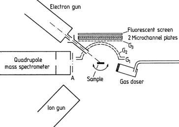
Schematic picture of an Electron Stimulated Desorption (ESD) and ESDIAD apparatus. The sample S can be rotated about an axis normal to the plane of the drawing. ESD ions are mass-analyzed in the quadrupole mass spectrometer, and ESDIAD patterns are displayed using the grid MicroChannel-Plate (MCP) plus fluorescent screen array. The radius of curvature of G 1 is 2 cm, and the active area of each MCP has a diameter of 4 cm. For most ESDIAD measurements typical potentials are G 1=G 2=0 V, G 3=−70 V, MCP entrance: −700 V, MCP midpoint: 0 V, MCP exit: +700 V, fluorescent screen: +3800 V. Electron gun filament potential V f=−100 V, crystal potential V B=0 to +100 V. Electron energy E e=e(|V f|+|V B|) [XVII.4]

The theoretical description of ESD processes is based on two limiting cases. In the classical model of Menzel and Gomer [XVII.5] intramolecular excitations (indicated by the shaded area in Fig. XVII.6) within the adsorbed molecule lead to non-bonding and antibonding neutral or ionic final states. At the crossover points of the corresponding potential curves (Fig. XVII.6) the adsorbed molecule can change into the new state and might desorb. In the case of ion desorption an electron can be captured by tunneling from the solid to a desorbing particle.

Potential energy diagrams for an adsorbate system. G: adsorbed ground state; M −+A +: ionic state; (M+A)∗: antibonding state; M+A ∗: excited state of the adsorbate; M ∗+A: adsorbate ground state with excitation energy in the metal (vertically shifted replica of G). The vibrational distribution in G and resulting ESD ion energy distribution are indicated [XVII.2]
This type of excitation, however, does not explain ESD results which have been observed on TiO2(001) surfaces on which tiny amounts of hydrogen were adsorbed (Fig. XVII.7) [XVII.6, XVII.7]. Under irradiation with quasi monoenergetic electrons of varying primary energy, thresholds in the desorption flux of H+ and O+ ions are observed near 21 eV and 34 eV, respectively. As is seen from additional double differentiated EELS measurements (inset), these energies correspond to the O(2s) and Ti(3p) core-level excitations. The interpretation of these desorption experiments on highly ionic materials involves the formation of core-level holes in the O(2s) and Ti(3p) orbitals and subsequent interatomic transitions between the O and Ti core levels. In detail, primary electrons create a Ti(3p) core hole, and owing to an interatomic Auger process an O(2p) electron decays into the Ti(3p) state, with the emission of a second or third O(2p) electron to dissipate the energy released in the decay. This fast process is responsible for the relatively large charge transfer in the transformation of the O2− lattice ion into O+, which is observed in ESD. The H+ desorption spectrum exhibiting two thresholds (Fig. XVII.7) may be interpreted in terms of two types of hydrogen, that bonded to O and that bonded to Ti surface atoms. Energy-dependent ESD measurements can thus give detailed information about atomic-scale features of the electron-induced desorption process.

(a), (b) Ion yields (O+,H+,OH+) from Electron-Stimulated Desorption (ESD) measurements on: (a) a clean annealed TiO2(001) surface (the H+ yield probably results from slight contamination); (b) an Ar-sputtered TiO2(001) surface after exposure to H2O. For comparison, part (a) contains as an insert a second-derivative Electron Energy Loss Spectrum (EELS) of the same annealed surface. Its loss scale (ΔE) is identical with the scale of the ESD primary energy. Transitions from the O(2s) and Ti(3p) levels to the vacuum level are indicated [XVII.6]
Experimental examples of the use of ESDIAD in the determination of an adsorption geometry are given in Fig. XVII.8. From TDS it is known that H2O and NH3, adsorb molecularly on the Ru(001) surface at 90 K. Irradiation by electrons with primary energies below 100 eV produces angularly-resolved desorption patterns of H+ ions, as shown in Figs. XVII.8(b)–(d) [XVII.4]. For low coverages a halo-type pattern is observed. Assuming that the desorbing H+ ions leave the surface along the direction of the intramolecular chemical bond, a low-coverage bonding geometry is derived in which the H2O and NH3 molecules are bonded with their O and N atoms closest to the surface. The orientation with respect to the 2D lattice planes of the surface is irregular or statistical. At increased coverages a hexagonal symmetry becomes visible in the ESDIAD patterns, which demonstrates that the molecular orientation is now in registry with the underlying substrate (Figs. XVII.8(c)–(e)). The molecules have lost one degree of freedom, the free rotation around an axis normal to the surface. With certain assumptions about the microscopic desorption process, ESDIAD thus allows detailed conclusions concerning the local adsorption geometry.

(a)–(e) Schematic ESDIAD patterns for H2O and NH3 adsorbed on Ru(001) at 90 K [XVII.4]. (a) Formation of hollow cone of H+ ions from adsorbed NH3 and H2O (at low coverages). (b) “Halo” H+ pattern characteristic of low coverages of NH3 and H2O. (c) Hexagonal H+ pattern characteristic of intermediate NH3 coverages (0.5≤θ<1). (d) Hexagonal H+ pattern characteristic of intermediate H2O coverages (0.2≤θ<1). (e) Ru(001) substrate with respect to the ESDIAD patterns above
References
-
XVII.1.
F.M. Lord, J.S. Kittelberger, Surf. Sci. 43, 173 (1974)
-
XVII.2.
D. Menzel, in Interactions on Metal Surfaces, ed. by R. Gomer. Topics Appl. Phys., vol. 4 (Springer, Berlin, 1974), p. 124
-
XVII.3.
F. Bozso, G. Ertl, M. Weiss, J. Catalysis 50, 519 (1977)
-
XVII.4.
T.E. Madey, J.T. Yates, Proc. 7th Int’l. Vac. Congr. and Int’l. Conf. Solid Surfaces (Wien, 1977)
-
XVII.5.
D. Menzel, R. Gomer, J. Chem. Phys. 41, 3311 (1964)
-
XVII.6.
M.L. Knotek, Surface Sci. 91, L17 (1980)
-
XVII.7.
M.L. Knotek, P.J. Feibelman, Phys. Rev. Lett. 40, 964 (1978)
Panel XVIII: Kelvin-Probe and Photoemission Measurements for the Study of Work-Function Changes and Semiconductor Interfaces
The adsorption of atoms or molecules on a solid surface, i.e. the first steps of the formation of a solid–solid interface, is generally associated with a change of work function (Sect. 10.3), and on semiconductors also with a change in band bending (because of the formation of new interface states). These effects can be studied in situ both by photoemission spectroscopy (UPS and XPS; Sect. 6.3) and by Kelvin-probe measurements. The latter technique, in particular, is useful for work-function measurements on metal surfaces, where space-charge layer effects are negligible (spatial extension of some Ångstroms).
Kelvin probes for the determination of work-function changes consist of an electrode (usually point-like) which can be positioned in front of the surface being studied (Fig. XVIII.1(a)). This counterelectrode is driven electromagnetically by a solenoid or by piezoceramics such that it vibrates with frequency ω against the sample surface. Sample and vibrating electrode are connected electrically through an ammeter (A) and a battery which allows a variable biasing (U comp).

(a) Principle of a Kelvin probe measurement; the compensation voltage U comp compensates the AC current driven by the vibrating probe. (b) Schematic circuit for the Kelvin probe measurement
The principle of the work-function measurement becomes clear if we consider that for two solids [sample S and probe P] in electrical contact the electrochemical potentials, i.e. the Fermi energies \(E_{\mathrm{F}}^{\mathrm{S}}\) and \(E_{\mathrm{F}}^{\mathrm{P}}\), are equal in thermal equilibrium (\(E_{\mathrm{F}}^{\mathrm{S}} = E_{\mathrm{F}}^{\mathrm{P}}\)). Since in general the work function (eϕ=E vac−E F) is different for the sample surface and for the Kelvin probe, a so-called contact potential U SP is built up between the sample and the probe.
Since
the contact potential is obtained as
Measurement of this contact potential therefore determines the difference in work function between the Kelvin probe and the sample surface. In an experimental set-up as in Fig. XVIII.1 the voltage between sample and probe is
The capacitor formed by sample and probe thus carries a charge (C being the capacitance)
and the vibration of the probe electrode (frequency ω) gives rise to an oscillating current
By means of the compensation voltage U comp the oscillating current I is compensated to zero and the particular value of U comp yields the difference in work function
For practical purposes Kelvin-probe measurements are usually performed by automatic compensating circuits, for example, of the type shown in Fig. XVIII.1(b). The AC current between sample and vibrating probe is amplified and detected phase-sensitively by a lock-in amplifier. The reference signal from the lock-in is also used to control the frequency of the AC voltage supplying the piezodrive. The DC output of the lock-in, which is proportional to its AC input amplitude, controls a variable voltage source which compensates the contact potential between sample surface and probe. The compensating voltage U comp is read out by a digital voltmeter and gives directly the required contact potential difference (XVIII.6).
If the work function eϕ P of the reference electrode (probe) is known, the work function of the sample surface is determined. The method is readily applicable if the sample surface can be covered by an adsorbate without affecting the probe surface. This can be achieved, e.g., if the Kelvin probe can be removed during evaporation onto the sample surface (with geometrically well-defined beam). Difficulties arise when adsorption from an ambient is studied and the probe surface is exposed to the same gas atmosphere. The accuracy of Kelvin probe measurements is quite high. Relative changes in ϕ S can be determined within error limits of about 10 meV. Absolute measurements, of course, depend on a knowledge of the work function of the probe. Absolute measurements are sometimes performed by means of comparison with well-defined surfaces for which the work function is known from other measurements. Two measurements are then needed, one on the known surface and one on the sample under study. The necessary exchange of the two samples in front of the Kelvin probe decreases the accuracy of the measurement considerably.
For semiconductor surfaces a knowledge of the work-function change eΔϕ=eϕ′−eϕ due to adsorption does not give direct insight into atomic properties. The work-function change contains contributions due to band-bending changes and in addition a surface dipole contribution which may be described as a change of the electron affinity χ. These two contributions can be determined separately in a photoemission experiment with UV light (UPS) or X-ray excitation (XPS). According to Fig. XVIII.2 an adsorption process giving rise to extrinsic Surface States (SS) in the gap and thus an upwards band bending (depletion layer) causes the work function eϕ to change into
where V S is the band bending (change in Fig. XVIII.2); eΔϕ Dip is a dipole contribution arising from the elemental dipoles of the adsorbed molecules or atoms (Δ) and may also include a change of the electron affinity \(\Delta\tilde{\chi}\) due to a surface reconstruction during adsorption
The distinction between Δ and \(\Delta\tilde{\chi}\) is rather arbitrary and can be avoided by using a single change of the electron affinity Δχ, such that the change in the work function due to adsorption is given as in (10.17a), (10.17b).

(a), (b) Explanation of adsorbate-induced changes in the photoemission spectrum of a semiconductor: (a) Photoemission process on the clean surface of a semiconductor. Photons of energy ħω excite electrons from the valence band (upper edge E V) into empty states, from where they leave the crystal and are detected with a kinetic energy above the vacuum energy E vac. True secondary electrons arise from multiple scattering events within the crystal. (b) An adsorbate induces extrinsic Surface States (SS) in the bulk band gap and an upwards band bending eV S. This changes the work function from eϕ to eϕ′. Simultaneously with the shift in valence and conduction band states, core level states also shift upwards in energy at the surface
Figure XVIII.2 is a schematic drawing of a photoemission experiment (UPS) in which electrons are emitted from occupied valence band states (of density given by shaded area) by irradiation with photons of energy ħω and detected with a kinetic energy E kin. The detected spectral distribution (also shaded) thus resembles the density of occupied states, but is superimposed on a background of true secondaries, which have undergone several inelastic processes on their way from the point of excitation to the solid surface. Since the probing depth in such an experiment is only a couple of Ångstroms (Sect. 6.3), small in comparison with the thickness of the space charge layer, the measured electron distribution yields information about the electronic band structure at the very surface. In the experiment the Fermi energy E F is the general reference point (chemical potential of electrically connected sample and analyser) and all measured energies are related to this. E F is usually determined at the end of the different measurements by evaporating a metal film onto the sample surface and determining the high energy onset of emission which, on a metal surface, is given by E F.
As is evident from Fig. XVIII.2 a change of work function eΔϕ=eϕ′−eϕ is directly detected as a change of the energy width of the entire spectral distribution of the emitted electrons. The exact position of the low energy flank of the true secondaries with respect to the experimentally determined position of E F gives the absolute values of the work functions eϕ with and without adsorbate present. In principle, both the work-function and the band-bending changes due to adsorption can be separately determined. The high-energy flank of the distribution of emitted electrons corresponds to the upper valence-band maximum (for normal emission). A shift of this flank due to adsorption indicates a shift of the valence-band edge with respect to the Fermi level and thus a band-bending change ΔV S (or V S for initially flat bands as in Fig. XVIII.2). This is only true if the adsorption process produces no new surface states in the gap. Such extrinsic gap states would modify the spectral distribution at the high-energy flank and the determination of any shift of the onset would be impossible. A second possibility for determining a band-bending change is via a characteristic emission band that is clearly recognized as due to bulk states (rather than surface states, Sect. 6.3.3). If this spectral band does not change its shape significantly upon adsorption (due to new surface states in the neighborhood), its position can be determined with sufficient accuracy on the clean surface and after adsorption. An observed shift gives direct information about the band bending change (Fig. XVIII.2). For example, the adsorption of metallic Sn on GaAs(110) surfaces has been studied by UPS in order to gain information about the Schottky-barrier formation (Fig. XVIII.3). The emission band near 4.7 eV binding energy (marked by an arrow) shifts to lower binding energy (i.e., towards the Fermi level E F) with increasing Sn coverage as does the emission onset corresponding to the upper valence band edge. This indicates an upwards band-bending change, i.e., the formation of a depletion layer on n-type material. A quantitative evaluation of the band bending is not possible from the shift of the emission onset since new metal-induced surface states cause a strong deformation of the spectrum. This is clearly seen from the plot in Fig. XVIII.4. The information about the band bending change must be extracted from the energetic position of the bulk emission band (filled circles).

UPS electron energy distribution curves of a clean (a) and Sn covered (b)–(d) n-GaAs(110) surface taken with He I radiation (hν=21.2 eV). The coverage θ is given in monolayers (1 ML contains 8.85⋅1014 atoms/cm2). The binding energy is defined relative to the energetic position of the valence band maximum at the clean surface. The arrow in spectrum (a) shows an emission band originating from bulk electronic states; its shift with coverage reflects the band bending change [XVIII.1]

Position of the high-energy emission onset of the UPS spectra of Fig. XVIII.3, relative to the position of the bulk valence-band maximum (open circles; left-hand ordinate) and energy shift of the GaAs valence-band emission peak (arrow in Fig. XVIII.3) at 4.7 eV below VBM (full circles; right-hand ordinate) versus Sn coverage for n-GaAs [XVIII.1]
A similar procedure for investigating band-bending changes upon adsorption can also be performed by XPS on core-level emission bands, since these shift in the same way as valence states (Fig. XVIII.2). Standard XPS equipment, however, does not usually offer sufficient energy resolution, and so optical monochromators are needed. Furthermore, severe problems in the analysis of the data can occur when chemical bonding shifts (Sect. 6.3) are superimposed on the band-bending shifts.
Photoemission spectroscopy, in particular UPS, also yields the most direct way to measure band offsets (discontinuities) (Sect. 8.1) in situ between different epitaxy steps. The principle of the method is explained in Fig. XVIII.5. On the same energy scale one plots the band structure of an uncompleted semiconductor heterostructure (a) together with the corresponding (kinetic) energy distribution of the emitted electrons (b). In an ideal case the clean surface spectrum of semiconductor I shows an emission onset which indicates the energetic position of its upper valence band maximum. After growing one or two monolayers of semiconductor II, a new shoulder appears whose emission onset characterizes the upper valence-band edge of semiconductor II. The difference between the two thresholds is simply the valence-band discontinuity. It is clear that this technique only works when the valence-band edge of semiconductor II occurs at energies higher than that of semiconductor I.

(a), (b) Qualitative explanation of the determination of semiconductor valence band offsets ΔE V by means of UV photoemission. On the clean surface of semiconductor I thin epitaxial layers of semiconductor II are grown (a) and the UPS spectra are measured in situ. (b) The shoulder II represents the valence band emission onset of semiconductor II on top of the valence band emission onset I of semiconductor I
Furthermore, the measurement can only be made on epilayers of thicknesses up to a couple of Ångstroms (information depth of UPS); but this is usually sufficient to allow the complete development of the band structure of semiconductor II. The method is illustrated in Fig. XVIII.6 for Ge overlayers on a ZnSe substrate [XVIII.2]. The energy of the new emission onset due to the Ge overlayer is insensitive to the crystallographic order of the Ge. An amorphous film exhibits the same band discontinuity as two other Ge overlayers which have been annealed and are crystalline.

ZnSe-Ge photoemission spectra showing the valence band offset ΔE V. These spectra were taken on unannealed, amorphous Ge overlayers (curve a) and on two different annealed Ge overlayers, exhibiting good LEED patterns (curves b and c). The spectra suggest that the order or disorder of the overlayer is not an important factor in ΔE V for this particular system [XVIII.2]
In general, it should be emphasized that photoemission techniques give quite direct information about band-bending changes, work function and band discontinuities; but the accuracy in determining the absolute values is typically between 20 and 100 meV. This is usually inadequate for narrow gap semiconductor such as InSb or InAs, in particular for explaining the electronic properties of interfaces.
References
-
XVIII.1.
M. Mattern-Klosson, H. Lüth, Surf. Sci. 162, 610 (1985)
-
XVIII.2.
G. Margaritondo, C. Quaresima, F. Patella, F. Sette, C. Capasso, A. Savoia, P. Perfetti, J. Vac. Sci. Technol. A 2, 508 (1984)
Problems
Problem 10.1
A cesium ion (Cs+) has an ionic radius of 3 Å. Calculate the approximate surface dipole moment for a (Cs+) ion adsorbed on a tungsten (W) surface and discuss the result with respect to the observed work-function changes for Cs-adsorption on a W surface (Fig. 10.12).
Problem 10.2
Calculate the time at which 10 % of the adsorption sites of a (100) W surface are occupied by nitrogen molecules, when the surface is exposed to an N2 pressure of 2.67⋅10−7 Pa at a temperature of 298 K. At this temperature the sticking probability is 0.55. The surface density of the adsorption sites amounts to 1⋅1015 cm−2.
Problem 10.3
Desorption studies of oxygen on tungsten (W) show that equal amounts of the gas are desorbed within 27 min at 1856 K, within 2 min at 1987 K and within 0.3 min at 2070 K. What is the activation energy for desorption of oxygen from W? What is the time needed for desorption of the sane amount of oxygen at the temperatures 298 K and 3000 K?
Problem 10.4
At 300 K, gas molecules have a sticking coefficient of S=0.1 on a freshly prepared, clean semiconductor surface. The adsorption is thermally activated with a sticking coefficient S∝exp(−E act/kT) and an activation energy per molecule of E act=0.1 eV. How high are the adsorbate coverages after a one hour exposure at 300 K and at 70 K, respectively? Are the adsorbate coverages detectable by Auger Electron Spectroscopy (AES)?
Rights and permissions
Copyright information
© 2015 Springer-Verlag Berlin Heidelberg
About this chapter
Cite this chapter
Lüth, H. (2015). Adsorption on Solid Surfaces. In: Solid Surfaces, Interfaces and Thin Films. Graduate Texts in Physics. Springer, Cham. https://doi.org/10.1007/978-3-319-10756-1_10
Download citation
DOI: https://doi.org/10.1007/978-3-319-10756-1_10
Publisher Name: Springer, Cham
Print ISBN: 978-3-319-10755-4
Online ISBN: 978-3-319-10756-1
eBook Packages: Physics and AstronomyPhysics and Astronomy (R0)